Lab 4 - EE 421L
Digital Integrated Circuit Design
Author:
Matthew Meza
Email:
mezam11@unlv.nevada.edu
September 21, 2015
IV characteristics and layout of NMOS
and PMOS
devices in ON's C5 process!
Pre-lab work
- Back-up all of your
work from
the lab and the course.
- Read through this
lab before
starting it.
- Go through Tutorial 2 seen here.
- In
the simulations in this lab
the body of all NMOS devices (the substrate) should be at ground (gnd!)
and
the body of all PMOS devices (the n-well) should be at a vdd! of
5V.
Lab Description
In
this lab we will layout an NMOS and PMOS MOSFET in ON's C5 Process.
After the layout, we will plot characterization
curves with different parameters! Layouts will include a probe/bond
pand!
Lab Requirement
- Lay out a 6u/0.6u
NMOS device
and connect all 4 MOSFET terminals to probe pads (which can be
considerably smaller than bond pads [see MOSIS
design rules] and
directly adjacent to the MOSFET (so the layout is relative small).
- Show your layout
passes
DRCs.
- Make a
corresponding schematic
so you can LVS your layout.
- Lay out a 12u/0.6u
PMOS device
and connect all 4 MOSFET terminals to probe pads.
- Show your layout
passes
DRCs.
- Make a
corresponding schematic
so you can LVS your layout
- Generate 4
schematics and simulations (see the examples in
the Ch6_IC61 library, but note that for the PMOS body should be at vdd!
instead of gnd!):
- A schematic for
simulating ID v. VDS of
an NMOS device
for VGS varying from 0 to 5 V in 1 V steps while VDS varies from 0 to 5
V in 1 mV steps. Use a 6u/600n width-to-length ratio.
- A schematic for
simulating ID v.
VGS of an NMOS device for VDS = 100 mV where VGS varies from 0 to 2 V
in 1 mV steps. Again use a 6u/600n width-to-length ratio.
- A schematic for
simulating ID v.
VSD (note VSD not VDS) of a PMOS device for VSG (not VGS) varying from
0 to 5 V in 1 V steps while VSD varies from 0 to 5 V in 1 mV steps.
Use a 12u/600n width-to-length ratio.
- A schematic for
simulating ID v.
VSG of a PMOS device for VSD = 100 mV where VSG varies from 0 to 2 V in
1 mV steps. Again, use a 12u/600n width-to-length ratio.
Post-Lab Excercises
NMOS Device!
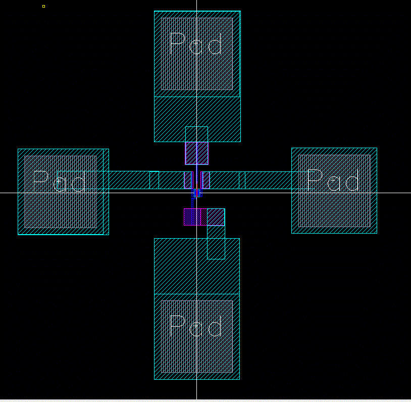 
Layout of the NMOS Device. Notice the four bond-pands (big squares)
The layout DRCs just fine!
|
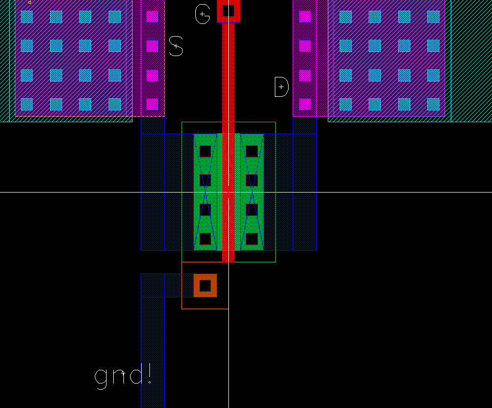
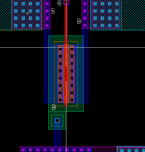
A close up of the layout. Shown is the NMOS device with
metal1 connected!
|
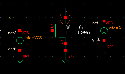
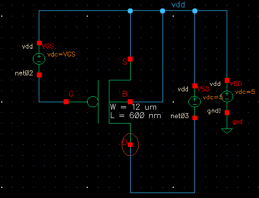
Schematic of the NMOS for simulation!
Parameters may change depending on the simulation.
|
 The layout and schematic netlists
match! The layout and schematic netlists
match!
Ready for simulation!
|
PMOS
Device!
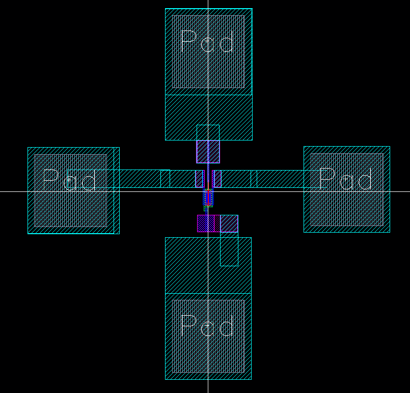 
Layout of the PMOS Device. Notice the four bond-pands (big squares)
The layout DRCs just fine!
|
A close up of the layout. Shown is the PMOS device with
metal1 connected!
|
Schematic of the PMOS for simulation!
Parameters may change depending on the simulation.
|
 The layout and schematic netlists
match! The layout and schematic netlists
match!
Ready for simulation!
|
Simulations!
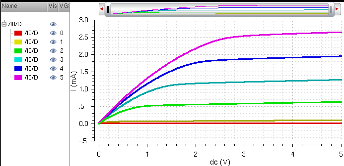
NMOS: ID vs VDS with VGS increments!
|
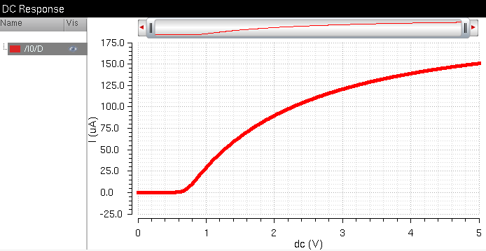
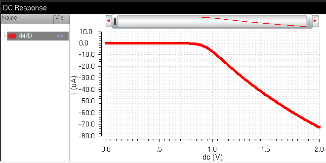
NMOS: ID vs VGS with VDS = 0.1 volts
|
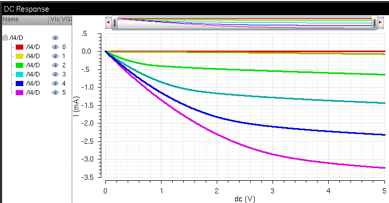
PMOS: ID vs VSD with VSG increments!
Notice how the waveform is flipped! This is because the
plot is displaying the current flowing INTO the drain!
|
PMOS: ID vs VSG with VDS = 0.1 volts
Notice how the waveform is flipped! Thisis because the
plot is displaying the current flowing INTO the drain!
|
Return
to EE 421 Labs